Logisim-Evolution
![]()
The latest, stable release Logisim-Evolution can be downloaded here. To help the project or try out the newest features & bug fixes, the nightly build can be used.
The installation process is easy to follow and the program can be used for digital logic design straight away.
If you encounter any issues, taking a look at the Wiki can be worth it, discussing it with the professor or open a new issue.
FPGA-tools path setup
Important
Before you can proceed with the setup, ensure that you have the CAD-tools installed on your machine as described in this section.
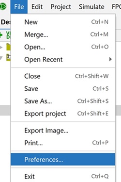
Click the
Filemenu and hitPreferencesto open the Preferences.
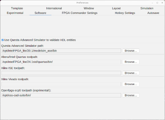
Select the
Softwaretab. To change the Openfpga ecp5 toolpath (experimental), click onBrowseand navigate to the binaries of the CAD-tools as indicated in the table below the image.
Operating system: |
VHDL-flow |
Verilog flow |
|---|---|---|
linux |
/opt/oss-cad-suite/bin/ |
/opt/oss-cad-suite/bin/ |
macOS |
/opt/oss-cad-suite/bin/ |
/opt/oss-cad-suite/bin/ |
Windows WSL |
/opt/oss-cad-suite/bin/ |
/opt/oss-cad-suite/bin/ |
Windows native |
not supported |
broken |
To select which flow to use:
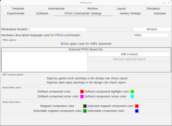
Select the
FPGA Commander Settings-tab and change the entry Hardware description used for FPGA-commander.
Downloading a logisim circuits to an FPGA
Downloading a circuit designed onto the FPGA is straight-forward with Logisim, but ensure that you have completed the previous step first.
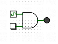
For this demonstration, a very basic design using a button as user input, a clock source, an AND gate, and finally a LED as user output.
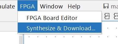
Navigate to the
FPGAmenu and click onSynthesize & Download.
The
Synhesize & Downloadwindow should open. First, configure the Target board to the GECKO5_EDUCATION board.
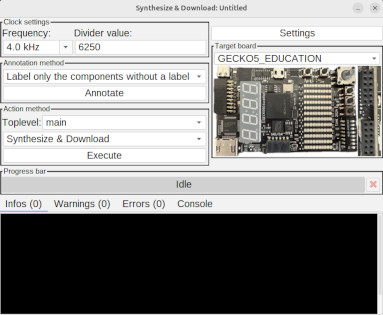
Note
The GECKO5_EDUCATION can be used for both the GECKO5Education as the GECKO5Modular. The only difference is that for the GECKO5Modular, the Pmod-interfaces are not available (right on the picture).
Using the
Frequencydrop-down menu, you can select the clock speed of the clock source in the logisim circuit. You can also set the clock settings by theDivider value, and use a fraction of the 50 MHz base clock.
Note
The frequency given here is the tick-frequency. As by default the clock source is one tick high and one tick low, this presents the double of the clock frequency.
Before the circuit can be synthesized, the input and output components need to be labeled, which can be done in the circuit editor. To ensure all components without a label are labeled, click
Annotate.To synthesize and load the design onto the FPGA board, click
ExecutewhileSynthesize & Downloadis selected in the Action method.Whenever
Synthesize & Downloadis executed, the user will be requested to check the component mapping window.
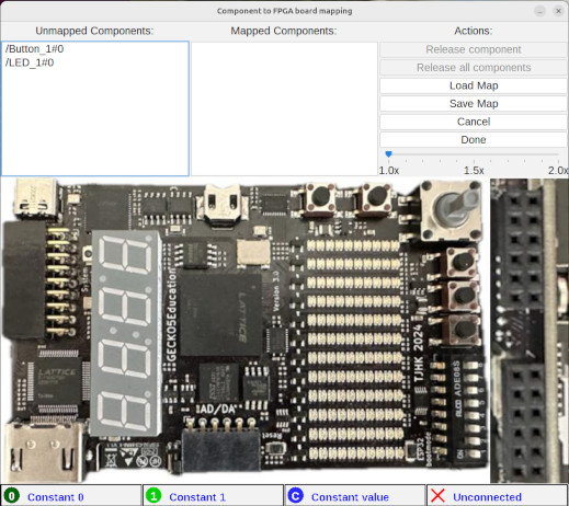
By clicking an unmapped component, the available input or output is highlighted on the FPGA board image. By clicking one of the dark-blue highlighted components on the image, the schematic component will be connected to the FPGA button, LED or I/O.
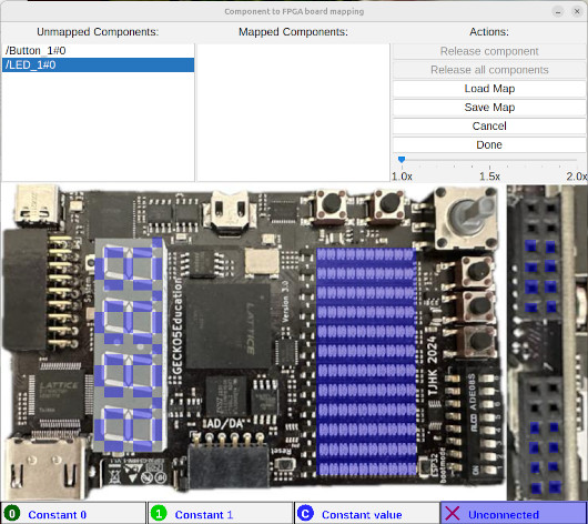
Once components are mapped, click
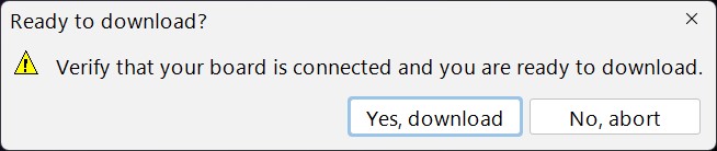
Doneto confirm and close the window. The synthesis will be done from here on and may take a short moment.After the circuit has been synthesized without errors, the following window will pop up. Ensure that the GECKO5Education/Modular is connected to the computer and hit
Yes, download.
The circuit will be downloaded onto the board and the LED should be blinking if the button is pressed.