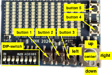
DIP-switch, buttons, and joystick

The GECKO5Education/Modular have an 8-position DIP-switch, 5 buttons, and a digital joystick. The naming conventions of these components is shown below:

buts

Using the DIP-switch, buttons, and/or joystick

In this section you find a VHDL and Verilog top-level and the corresponding lpf-file that you can use for the different elements.

Important

Although VHDL is case-insensitive, the lpf-file is not. Meaning that the port-names in the top-level entity need to be copied exactly in the lpf-file.

An example for a VHDL top-level entity is shown below:

library ieee;
use ieee.std_logic_1164.all;

entity toplevel is
  port ( nButtons   : in std_logic_vector( 4 downto 0 );
         nJoystick  : in std_logic_vector( 4 downto 0 );
         nDipSwitch : in std_logic_vector( 7 downto 0 );
         ... );
end toplevel;

An example for a Verilog top-level is shown below:

module toplevel (
  input wire [4:0] nButtons,
                   nJoystick,
  input wire [7:0] nDipSwitch,
  ...);
  ...
endmodule

The required entries in the lpf-file are:

LOCATE COMP "nButtons[0]" SITE "M18";
LOCATE COMP "nButtons[1]" SITE "M17";
LOCATE COMP "nButtons[2]" SITE "L18";
LOCATE COMP "nButtons[3]" SITE "J18";
LOCATE COMP "nButtons[4]" SITE "J17";
IOBUF PORT "nButtons[0]" PULLMODE=UP IO_TYPE=LVCMOS18;
IOBUF PORT "nButtons[1]" PULLMODE=UP IO_TYPE=LVCMOS18;
IOBUF PORT "nButtons[2]" PULLMODE=UP IO_TYPE=LVCMOS18;
IOBUF PORT "nButtons[3]" PULLMODE=UP IO_TYPE=LVCMOS18;
IOBUF PORT "nButtons[4]" PULLMODE=UP IO_TYPE=LVCMOS18;

LOCATE COMP "nJoystick[0]" SITE "L17";
LOCATE COMP "nJoystick[1]" SITE "K19";
LOCATE COMP "nJoystick[2]" SITE "K18";
LOCATE COMP "nJoystick[3]" SITE "N16";
LOCATE COMP "nJoystick[4]" SITE "N17";
IOBUF PORT "nJoystick[0]" PULLMODE=UP IO_TYPE=LVCMOS18;
IOBUF PORT "nJoystick[1]" PULLMODE=UP IO_TYPE=LVCMOS18;
IOBUF PORT "nJoystick[2]" PULLMODE=UP IO_TYPE=LVCMOS18;
IOBUF PORT "nJoystick[3]" PULLMODE=UP IO_TYPE=LVCMOS18;
IOBUF PORT "nJoystick[4]" PULLMODE=UP IO_TYPE=LVCMOS18;

LOCATE COMP "nDipSwitch[0]" SITE "D19";
LOCATE COMP "nDipSwitch[1]" SITE "D17";
LOCATE COMP "nDipSwitch[2]" SITE "J16";
LOCATE COMP "nDipSwitch[3]" SITE "H16";
LOCATE COMP "nDipSwitch[4]" SITE "C20";
LOCATE COMP "nDipSwitch[5]" SITE "C18";
LOCATE COMP "nDipSwitch[6]" SITE "D18";
LOCATE COMP "nDipSwitch[7]" SITE "D20";
IOBUF PORT "nDipSwitch[0]" PULLMODE=UP IO_TYPE=LVCMOS18;
IOBUF PORT "nDipSwitch[1]" PULLMODE=UP IO_TYPE=LVCMOS18;
IOBUF PORT "nDipSwitch[2]" PULLMODE=UP IO_TYPE=LVCMOS18;
IOBUF PORT "nDipSwitch[3]" PULLMODE=UP IO_TYPE=LVCMOS18;
IOBUF PORT "nDipSwitch[4]" PULLMODE=UP IO_TYPE=LVCMOS18;
IOBUF PORT "nDipSwitch[5]" PULLMODE=UP IO_TYPE=LVCMOS18;
IOBUF PORT "nDipSwitch[6]" PULLMODE=UP IO_TYPE=LVCMOS18;
IOBUF PORT "nDipSwitch[7]" PULLMODE=UP IO_TYPE=LVCMOS18;

Important

  1. Note the case-sensitivity of the lpf-file.

  2. The tools require exactly one lpf-file, hence all assignments you use need to be in a single lpf-file.

  3. All elements must have specified the PULLMODE=UP. As there are no pull-up resistors on board, failing to do so will result in non-functional elements.

Note

All elements are active-low: when activated they will produce a logic 0, otherwise they provide a logic 1.

The below table shows the bit-mapping of the signal nButtons:

bit 0:

bit 1:

bit 2:

bit 3:

bit 4:

button 1

button 2

button 3

button 4

button 5

The below table shows the bit-mapping of the signal nJoystick:

bit 0:

bit 1:

bit 2:

bit 3:

bit 4:

left

down

right

up

center

The below table shows the bit-mapping of the signal nDipSwitch:

bit 0:

bit 1:

bit 2:

bit 3:

bit 4:

bit 5:

bit 6:

bit 7:

switch 1

switch 2

switch 3

switch 4

switch 5

switch 6

switch 7

switch 8

Summary

Below the table with all required information for the buttons:

Name:

FPGA pin:

IO_Type:

Pull up/down:

Active low/high:

button 1

M18

LVCMOS18

UP

active low

button 2

M17

LVCMOS18

UP

active low

button 3

L18

LVCMOS18

UP

active low

button 4

J18

LVCMOS18

UP

active low

button 5

J17

LVCMOS18

UP

active low

Below the table with all required information for the joystick:

Name:

FPGA pin:

IO_Type:

Pull up/down:

Active low/high:

up

N16

LVCMOS18

UP

active low

down

K19

LVCMOS18

UP

active low

left

L17

LVCMOS18

UP

active low

right

K18

LVCMOS18

UP

active low

center

N17

LVCMOS18

UP

active low

Below the table with all required information for the DIP-switch:

Name:

FPGA pin:

IO_Type:

Pull up/down:

Active low/high:

switch 1

D19

LVCMOS18

UP

active low

switch 2

D17

LVCMOS18

UP

active low

switch 3

J16

LVCMOS18

UP

active low

switch 4

H16

LVCMOS18

UP

active low

switch 5

C20

LVCMOS18

UP

active low

switch 6

C18

LVCMOS18

UP

active low

switch 7

D18

LVCMOS18

UP

active low

switch 8

D20

LVCMOS18

UP

active low