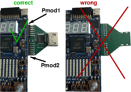
Pmod interfaces
The GECKO5Education provides two dual-row Digilent Pmod interfaces. These interfaces provide 16 general purpose I/O’s to be able to connect extensions to the GECKO5Education. Although in the Pmod-interface specification the connectors are placed on the top-side of the board, the GECKO5Education provides them on the bottom-side. The correct connection of a Pmod-module to the GECKO5Education is shown below:
Note
The Pmod-interfaces on the GECKO5Education are based on 3.3V I/O, meaning that: \(\text{V}_\text{CC}=3.3\text{V}\)
Using the Pmod interfaces
In this section you find a VHDL and Verilog top-level and the corresponding lpf-file that you can use for the Pmod interfaces.
Important
Although VHDL is case-insensitive, the lpf-file is not. Meaning that the port-names in the top-level entity need to be copied exactly in the lpf-file.
An example for a VHDL top-level entity is shown below:
library ieee;
use ieee.std_logic_1164.all;

entity toplevel is
  port ( pmod1P1  : inout std_logic;
         pmod1P2  : inout std_logic;
         pmod1P3  : inout std_logic;
         pmod1P4  : inout std_logic;
         pmod1P7  : inout std_logic;
         pmod1P8  : inout std_logic;
         pmod1P9  : inout std_logic;
         pmod1P10 : inout std_logic;
         pmod2P1  : inout std_logic;
         pmod2P2  : inout std_logic;
         pmod2P3  : inout std_logic;
         pmod2P4  : inout std_logic;
         pmod2P7  : inout std_logic;
         pmod2P8  : inout std_logic;
         pmod2P9  : inout std_logic;
         pmod2P10 : inout std_logic;
         ... );
end toplevel;
An example for a Verilog top-level is shown below:
module toplevel (
  inout wire pmod1P1,
             pmod1P2,
             pmod1P3,
             pmod1P4,
             pmod1P7,
             pmod1P8,
             pmod1P9,
             pmod1P10,
             pmod2P1,
             pmod2P2,
             pmod2P3,
             pmod2P4,
             pmod2P7,
             pmod2P8,
             pmod2P9,
             pmod2P10,
  ...);
  ...
endmodule
The required entries in the lpf-file are:
LOCATE COMP "pmod1P1" SITE "C3";
LOCATE COMP "pmod1P2" SITE "C4";
LOCATE COMP "pmod1P3" SITE "D5";
LOCATE COMP "pmod1P4" SITE "C5";
LOCATE COMP "pmod1P7" SITE "E3";
LOCATE COMP "pmod1P8" SITE "E4";
LOCATE COMP "pmod1P9" SITE "D3";
LOCATE COMP "pmod1P10" SITE "E5";
LOCATE COMP "pmod2P1" SITE "C1";
LOCATE COMP "pmod2P2" SITE "C2";
LOCATE COMP "pmod2P3" SITE "B2";
LOCATE COMP "pmod2P4" SITE "B1";
LOCATE COMP "pmod2P7" SITE "E1";
LOCATE COMP "pmod2P8" SITE "E2";
LOCATE COMP "pmod2P9" SITE "D1";
LOCATE COMP "pmod2P10" SITE "D2";
IOBUF PORT "pmod1P1" PULLMODE=NONE IO_TYPE=LVCMOS33;
IOBUF PORT "pmod1P2" PULLMODE=NONE IO_TYPE=LVCMOS33;
IOBUF PORT "pmod1P3" PULLMODE=NONE IO_TYPE=LVCMOS33;
IOBUF PORT "pmod1P4" PULLMODE=NONE IO_TYPE=LVCMOS33;
IOBUF PORT "pmod1P7" PULLMODE=NONE IO_TYPE=LVCMOS33;
IOBUF PORT "pmod1P8" PULLMODE=NONE IO_TYPE=LVCMOS33;
IOBUF PORT "pmod1P9" PULLMODE=NONE IO_TYPE=LVCMOS33;
IOBUF PORT "pmod1P10" PULLMODE=NONE IO_TYPE=LVCMOS33;
IOBUF PORT "pmod2P1" PULLMODE=NONE IO_TYPE=LVCMOS33;
IOBUF PORT "pmod2P2" PULLMODE=NONE IO_TYPE=LVCMOS33;
IOBUF PORT "pmod2P3" PULLMODE=NONE IO_TYPE=LVCMOS33;
IOBUF PORT "pmod2P4" PULLMODE=NONE IO_TYPE=LVCMOS33;
IOBUF PORT "pmod2P7" PULLMODE=NONE IO_TYPE=LVCMOS33;
IOBUF PORT "pmod2P8" PULLMODE=NONE IO_TYPE=LVCMOS33;
IOBUF PORT "pmod2P9" PULLMODE=NONE IO_TYPE=LVCMOS33;
IOBUF PORT "pmod2P10" PULLMODE=NONE IO_TYPE=LVCMOS33;
Important
Note the case-sensitivity of the lpf-file.
The tools require exactly one lpf-file, hence all assignments you use need to be in a single lpf-file.
Note
In the code snippets above all signals are defined as inout. The direction of these pins is dependent on the Pmod-module attached to the Pmod-interface.
Summary
Below the table with all required information for the Pmod-interface:
Name: |
FPGA pin: |
IO_TYPE: |
Name: |
FPGA pin: |
IO_TYPE: |
|---|---|---|---|---|---|
Pmod 1 Pin 1 |
C3 |
LVCMOS33 |
Pmod 1 Pin 7 |
E3 |
LVCMOS33 |
Pmod 1 Pin 2 |
C4 |
LVCMOS33 |
Pmod 1 Pin 8 |
E4 |
LVCMOS33 |
Pmod 1 Pin 3 |
D5 |
LVCMOS33 |
Pmod 1 Pin 9 |
D3 |
LVCMOS33 |
Pmod 1 Pin 4 |
C5 |
LVCMOS33 |
Pmod 1 Pin 10 |
E5 |
LVCMOS33 |
Pmod 2 Pin 1 |
C1 |
LVCMOS33 |
Pmod 2 Pin 7 |
E1 |
LVCMOS33 |
Pmod 2 Pin 2 |
C2 |
LVCMOS33 |
Pmod 2 Pin 8 |
E2 |
LVCMOS33 |
Pmod 2 Pin 3 |
B2 |
LVCMOS33 |
Pmod 2 Pin 9 |
D1 |
LVCMOS33 |
Pmod 2 Pin 4 |
B1 |
LVCMOS33 |
Pmod 2 Pin 10 |
D2 |
LVCMOS33 |