A/D and D/A converters
The GECKO5Education/Modular contain a 2-channel SPI-based Analog-to-Digital (A/D), and a 2-channel SPI-based Digital-to-Analog (D/A) converter. The D/A converter is a LTC2632. On the black EPFL-edition the A/D converter is a MAX11666. The blue MSE/BME edition uses a MAX11102.
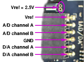
The image above shows the analog connections of the A/D and D/A converter.
Using the A/D and/or D/A converters
In this section you find a VHDL and Verilog top-level and the corresponding lpf-file that you can use for the A/D and D/A converters.
Important
Although VHDL is case-insensitive, the lpf-file is not. Meaning that the port-names in the top-level entity need to be copied exactly in the lpf-file.
An example for a VHDL top-level entity is shown below:
library ieee;
use ieee.std_logic_1164.all;

entity toplevel is
  port ( adcDacSclk : out std_logic;
         dacNCs     : out std_logic;
         dacSdi     : out std_logic;
         adcNCs     : out std_logic;
         adcChanSel : out std_logic;
         adcSdo     : in  std_logic;
         ... );
end toplevel;
An example for a Verilog top-level is shown below:
module toplevel (
  output wire adcDacSclk,
              dacNCs,
              dacSdi,
              adcNCs,
              adcChanSel,
  input wire  adcSdo,
  ...);
  ...
endmodule
The required entries in the lpf-file are:
LOCATE COMP "adcDacSclk" SITE "A13";
LOCATE COMP "dacNCs" SITE "B16";
LOCATE COMP "dacSdi" SITE "A16";
LOCATE COMP "adcNCs" SITE "E12";
LOCATE COMP "adcChanSel" SITE "A12";
LOCATE COMP "adcSdo" SITE "A14";
IOBUF PORT "adcDacSclk" PULLMODE=NONE IO_TYPE=LVCMOS33;
IOBUF PORT "dacNCs" PULLMODE=NONE IO_TYPE=LVCMOS33;
IOBUF PORT "dacSdi" PULLMODE=NONE IO_TYPE=LVCMOS33;
IOBUF PORT "adcNCs" PULLMODE=NONE IO_TYPE=LVCMOS33;
IOBUF PORT "adcChanSel" PULLMODE=NONE IO_TYPE=LVCMOS33;
IOBUF PORT "adcSdo" PULLMODE=NONE IO_TYPE=LVCMOS33;
Important
Note the case-sensitivity of the lpf-file.
The tools require exactly one lpf-file, hence all assignments you use need to be in a single lpf-file.
Voltage reference
To be able to operate the A/D and D/A converters they require a voltage reference \(\text{V}_\text{ref}\). The voltage range of this voltage reference is: \(1\text{V} \le \text{V}_\text{ref} \le 3.3\text{V}\). In case the A/D and D/A converters are not configured, there is no voltage reference. To provide a voltage reference there are three possibilities:
The D/A converter can be configured to put it’s internal voltage reference on the \(\text{V}_\text{ref}\)-pin. This is the prefered way.
By shorting the jumper marked as \(\text{V}_\text{ref} = 2.5\text{V}\) in the above image, the reference voltage is fixed to 2.5V.
The user can also put a reference voltage on the pin marked as \(\text{V}_\text{ref}\) in the above image.
Important
In case of using the 2.5V or user voltage, make sure that you never configure the D/A converter to put it’s internal voltage on the \(\text{V}_\text{ref}\)-pin, as this will distroy the D/A converter.
Summary
Below the table with all required information for the A/D and D/A converter:
Name: |
FPGA pin: |
IO_TYPE: |
Active low/high |
Description: |
|---|---|---|---|---|
A/D D/A Sclk |
A13 |
LVCMOS33 |
active high |
Shared serial clock |
D/A chip select |
B16 |
LVCMOS33 |
active low |
Enable the SPI bus of the D/A |
D/A data out |
A16 |
LVCMOS33 |
active high |
D/A serial data line |
A/D chip select |
E12 |
LVCMOS33 |
active low |
Enable the SPI bus of the A/D |
A/D channel select |
A12 |
LVCMOS33 |
active high |
Selects the analog channel |
A/D data in |
A14 |
LVCMOS33 |
active high |
A/D serial data line |