Camera interface
The GECKO5Education/Modular contains a camera interface. This interface is designed to hold an Olimex CAMERA-OV7670 module. But of course also other camera’s and/or add-on modules can be attached to this interface, as long as they are pin-compatible.
This connector contains basically an \(\text{I}^2\text{C}\)-interface and an eight-bit parallel pixel interface.
Important
When using the Olimex module, make sure to connect it to the GECKO5Education/Modular before connecting it to your computer! Failing to do so may result in breaking your camera module!
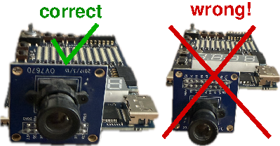
Make sure you connect the camera module correctly, hence the camera should look out on the top-side of the GECKO5Education/Modular (see below).
When using another camera as the Olimex module, make sure that the \(\text{I}^2\text{C}\)-slave-addresses are not 0xD0/0xD1, as these are used by the Real-Time-Clock.
Camera interface pin out
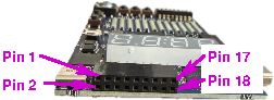
The pin-definitions of the camera-connector are listed below:
Pin Nr.: |
Function: |
Direction: |
Pin Nr.: |
Function: |
Direction: |
|---|---|---|---|---|---|
1 |
Ground |
Power |
10 |
Data bit 7 |
Input |
2 |
3.3 V |
Power |
11 |
Data bit 4 |
Input |
3 |
SDA |
Bidir |
12 |
Data bit 5 |
Input |
4 |
SCL |
Output |
13 |
Data bit 2 |
Input |
5 |
Hor. Sync. |
Input |
14 |
Data bit 3 |
Input |
6 |
Vert. Sync. |
Input |
15 |
Data bit 0 |
Input |
7 |
24 MHz clock |
Output |
16 |
Data bit 1 |
Input |
8 |
Pixel clock |
Input |
17 |
GND |
Power |
9 |
Data bit 6 |
Input |
18 |
Sys. Reset# |
Output |
Important
The \(\text{I}^2\text{C}\)-interface (SDA and SCL) must be preserved, as also the Real-Time-Clock (RTC) is connected to this bus!
Note
The direction is seen from the FPGA.
Pin 7 is driven by a 24 MHz oscillator (3.3V).
Pin 18 is an active-low system reset pin driven by the board (3.3V).
Using the camera interface
In this section you find a VHDL and Verilog top-level and the corresponding lpf-file that you can use for the camera interface.
Note
Make sure that in case you also use the Real-Time-Clock you only define the \(\text{I}^2\text{C}\)-interface once!
Important
Although VHDL is case-insensitive, the lpf-file is not. Meaning that the port-names in the top-level entity need to be copied exactly in the lpf-file.
An example for a VHDL top-level entity is shown below:
library ieee;
use ieee.std_logic_1164.all;

entity toplevel is
  port ( scl        : out   std_logic;
         sda        : inout std_logic;
         hsync      : in    std_logic;
         vsync      : in    std_logic;
         pixelClock : in    std_logic;
         pixelData  : in    std_logic_vector( 7 downto 0);
         ...);
end toplevel;
An example for a Verilog top-level is shown below:
module toplevel (
  output wire      scl,
  inout  wire      sda,
  input  wire      hsync,
                   vsync,
                   pixelClock,
  input wire [7:0] pixelData,
  ...);
  ...
endmodule
The required entries in the lpf-file are:
LOCATE COMP "scl" SITE "P3";
LOCATE COMP "sda" SITE "K2";
LOCATE COMP "pixelClock" SITE "H2";
LOCATE COMP "hsync" SITE "J1";
LOCATE COMP "vsync" SITE "H1";
LOCATE COMP "pixelData[0]" SITE "P2";
LOCATE COMP "pixelData[1]" SITE "P1";
LOCATE COMP "pixelData[2]" SITE "N2";
LOCATE COMP "pixelData[3]" SITE "N1";
LOCATE COMP "pixelData[4]" SITE "L1";
LOCATE COMP "pixelData[5]" SITE "M1";
LOCATE COMP "pixelData[6]" SITE "K1";
LOCATE COMP "pixelData[7]" SITE "L2";
IOBUF PORT "scl" PULLMODE=UP IO_TYPE=LVCMOS33;
IOBUF PORT "sda" PULLMODE=UP IO_TYPE=LVCMOS33;
IOBUF PORT "pixelClock" PULLMODE=NONE IO_TYPE=LVCMOS33;
IOBUF PORT "hsync" PULLMODE=NONE IO_TYPE=LVCMOS33;
IOBUF PORT "vsync" PULLMODE=NONE IO_TYPE=LVCMOS33;
IOBUF PORT "pixelData[0]" PULLMODE=NONE IO_TYPE=LVCMOS33;
IOBUF PORT "pixelData[1]" PULLMODE=NONE IO_TYPE=LVCMOS33;
IOBUF PORT "pixelData[2]" PULLMODE=NONE IO_TYPE=LVCMOS33;
IOBUF PORT "pixelData[3]" PULLMODE=NONE IO_TYPE=LVCMOS33;
IOBUF PORT "pixelData[4]" PULLMODE=NONE IO_TYPE=LVCMOS33;
IOBUF PORT "pixelData[5]" PULLMODE=NONE IO_TYPE=LVCMOS33;
IOBUF PORT "pixelData[6]" PULLMODE=NONE IO_TYPE=LVCMOS33;
IOBUF PORT "pixelData[7]" PULLMODE=NONE IO_TYPE=LVCMOS33;
FREQUENCY PORT "pixelClock" 12 MHZ;
Important
Note the case-sensitivity of the lpf-file.
The tools require exactly one lpf-file, hence all assignments you use need to be in a single lpf-file.
Note
The pixelClock with a frequency of 12 MHz is in case of 640x480, 15 FPS, and RGB565 for the Olimex camera. You need to modify it for your requirements.
The \(\text{I}^2\text{C}\)-interface is an open-collector/drain interface, hence a logic 0 is forced, and a logic 1 is realized with a pull-up.
Using the Olimex CAMERA-OV7670 module
The data sheet for this module can be found here. In the course CS-476: Embedded System Design at EPFL we use the camera in the configuration 640x480 pixels, 15 Frames Per Second (FPS), and a RGB565 data-format.
To be able to use the camera with these settings, it needs to be initialized through the \(\text{I}^2\text{C}\)-interface at start-up. The \(\text{I}^2\text{C}\)-address for writing to the camera is 0x42, and reading from it is 0x43.
The code used is based on this nice project for the Arduino-uno on GitHub. It was modified to account for the given system of the course.
Summary
Below a table with all required information for the \(\text{I}^2\text{C}\)-interface, shared between the camera and Real-Time-Clock:
Name : |
FPGA pin: |
IO_TYPE: |
Pull-up/down: |
|---|---|---|---|
SCL |
P3 |
LVCMOS33 |
UP |
SDA |
K2 |
LVCMOS33 |
UP |
Below the table with all required information for the pixel-interface of the camera:
Name: |
FPGA pin: |
IO_TYPE: |
Pull-up/down: |
Name: |
FPGA pin: |
IO_TYPE: |
Pull-up/down: |
|---|---|---|---|---|---|---|---|
pixel clock |
H2 |
LVCMOS33 |
NONE |
||||
horizontal sync |
J1 |
LVCMOS33 |
NONE |
vertical sync |
H1 |
LVCMOS33 |
NONE |
pixel data 0 |
P2 |
LVCMOS33 |
NONE |
pixel data 1 |
P1 |
LVCMOS33 |
NONE |
pixel data 2 |
N2 |
LVCMOS33 |
NONE |
pixel data 3 |
N1 |
LVCMOS33 |
NONE |
pixel data 4 |
L1 |
LVCMOS33 |
NONE |
pixel data 5 |
M1 |
LVCMOS33 |
NONE |
pixel data 6 |
K1 |
LVCMOS33 |
NONE |
pixel data 7 |
L2 |
LVCMOS33 |
NONE |